Semiconductor and Electronics
WAFERS
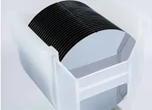
Silicon Nitride Wafers
Ovitech and its partners has developed temporary materials and carrier. Traditional temporary bonding adhesives for wafer processing have always required a carrier to match carrier-device wafer CTE during the rigors of processing. By eliminating the traditional glass carrier or silicon wafer carrier, wafer per hour throughput is greatly increased.
To successfully enable wafer processing with disposable carrier the key is the innovative, molecularly engineered temporary bonding adhesive: highly conforming, stretchable, and flexible temporary bonding adhesive yet with high shear bonding strength and high-temperature stability.
** Minimum batch order of 25 wafers.
PECVD silicon nitride layers allow higher growth rate, which therefore leads to thicker layers. Stoichiometry and stress can also be adjusted. High thickness uniformity and etch rates are eventually obtained. PECVD Silicon nitride wafers are particularly suitable for passivation layers.

Dummy Wafers
Wafer size: 100 / 150 / 200 / 300 mm
Services:
Polishing / Film Removing / Pattern Removal
Warpage / Crystal Orientation Measurement
Wafer surface inspection ( Scratches / edge chips / film / crack / slip )/
P/N TYPE / Electric Resistance / TTV / BOW / Warpage

Reclaim Wafers
Wafer size: 100 / 150 / 200 / 300 mm
Services:
Polishing / Film Removing / Pattern Removal
Warpage/ Crystal Orientation Measurement
Wafer surface inspection( Scratches / edge chips / film / crack / slip) / P/N TYPE / Electric resistance / TTV / BOW / Warpage
Particle control :0.3μm / 0.2μm / 0.12μm / 90 nm / 60 nm / 40 nm / 32 nm
COA : base on customers’ requirements including particle control
